Designing an Opamp Headphone Amplifier
(A HeadWize
Design Series Paper)
Because a few milliwatts will drive headphones to full volume, a great headphone amplifier
design can be relatively simple. Yet, there are any number of reasons for experimenting
with more complex topologies, such as improved performance and the ability to incorporate
custom options. Of course, some DIYers like to try different circuits just for the fun of
it. The major disadvantage of complex circuits is that they are complex. It can take a
DIYer months to locate and purchase the parts, not to mention the time to assemble and
troubleshoot the project.
Integrated circuit opamps are both complex and simple. They may contain hundreds of components on a chip, but are relatively easy to configure. For DIYers short on time and patience (and few people have the luxury of both), opamps are a convenient entre into the world of complex design. The audio cognescenti have attacked opamps as being one of the major causes of "mid-fi" sound, but if the truth be known, they are lurking everywhere - even under the covers of prestigious high-end gear. Opamps are not all the same. Building a headphone amplifier with good sound is a matter of careful selection and design.
This article discusses several opamp-based headphone amplifier circuits, including suggestions for selecting opamps, input coupling and filtering, high current output stages and power supply options. There are no recommendations for specific opamp brands or models. For tube devotees, there is also an introduction to designing with tube amp-blocks. Tube amp-blocks (AC feedback amplifiers and tube opamps) are not as compact as their silicon brethren, nor do they measure as well, but they do offer smooth tube sound with the ease of feedback configuration.
SELECTING SOLID STATE OPAMPS
Entire books cover the subject of interpreting opamp specifications. Here are a few guidelines for choosing opamps when designing headphone amplifiers. Opamps inch closer to the "ideal" with every succeeding generation. Modern devices are internally compensated for stability, have slew rates going through the roof and noise and distortion numbers at threshold of measurement. There are even opamps that will run off a 1-volt supply. For portable devices, the power supply requirements should be the first consideration. The majority of modern opamps will run with as little as ±4V, but low voltages may degrade performance. Check the manufacturer's VCC specs to confirm that low voltage operation is, in fact, recommended. The most common battery supply voltages are ±1.5V, ±3V, ±4.5V and ±9V. Single supplies are another possibility. Keep in mind also that the idling current for the entire amplifier must also be low - around 10mA or less for good battery life. For more information, see the section on battery power options below.
Opamp performance specifications are an unreliable indicator of sound quality. So long as the numbers are below audibility thresholds, specs that are magnitudes better than the averages will not necessarily translate into better sound. Regardless of type (bipolar or FET), modern opamps do very well on the test bench. Total harmonic distortion figures are so low (typically less than 0.1%) that datasheets have stopped listing them. Look for noise specifications, listed as "noise density" in units of nV/
Ö(Hz), of 25 or less, slew rates of 5uV/sec or more and "wide" unity gain-bandwidths of 3 MHz and higher.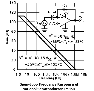
Figure 1a
When reviewing the gain-bandwidth specification of a bipolar-input opamp, also examine the open-loop bandwidth. The gain-bandwidth defines the amount of small-signal gain at any frequency and is the product of the open-loop bandwidth and the open-loop gain. Most opamps have a high open-loop gain (100dB or more) and a relatively narrow open-loop bandwidth (100Hz or less). In a multi-stage system with overall feedback, if the opamp has a bipolar input stage and narrow open-loop bandwidth, it can manifest dynamic phase shifts and other response non-linearities with high level, high frequency input signals.
To reduce this type of distortion, choose a bipolar-input opamp with a wide open-loop bandwidth (into the kHz range) or use a FET-input opamp. FET input stages are more linear and so less susceptible to this type of distortion. Finally, the open-loop bandwidth of the voltage-gain input stage can be effectively extended with local feedback (see the section on output stages below).
Also look for unity gain stability and low offset voltage. Opamps that are internally compensated are less likely to oscillate at high frequencies, and save the builder the hassle of adding external compensation (however, it never hurts to check the amplifier output on an oscilloscope anyway.) The ideal opamp has zero DC output at idle, so that DC coupling can be accomplished without trimming. Real-world opamps have a small output voltage at idle. If the opamp is not followed by a gain stage, a 15mV or less offset at idle should be acceptable. FET-input opamps are known for their low offset voltages.
Are there audible differences between opamps with similar or identical specs? Some listeners can distinguish between products, but not all. Because modern opamps are internally compensated and are usually plug-in replacements for each other, building circuits with IC sockets or on protoboard first allows the DIYer to audition a variety of opamps at will. Theories abound as to why opamps may have sonic signatures in spite of stellar test results that suggest neutral sound. Years ago, IM, DIM, TIM, etc. distortion were held to be the culprits. Two of the most recent courses of research on this topic have been the effects of the harmonic structure of opamp noise and opamp input errors.
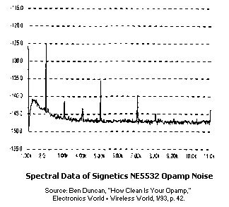
Figure 1b
Figure 1b is a plot of the noise spectrum of a common bipolar-input opamp. Noise structures with a predominance of even harmonics seem to sound less harsh. Manufacturers generally do not include such analyses in datasheets. Since these tests must be done with sophisticated equipment that can measure noise 140dB or more below the signal, most DIYers will have to rely on other published sources for this type of data.
There are three types of opamp input errors that potentially affect sound quality: source-impedance, power-supply and thermal errors due to the output loading of an opamp. Source-impedance errors arise when there are unequal source impedances at each of the two inputs to an opamp, which interact with the opamp's internal capacitances to create even-order harmonic distortion. It is a common-mode type error, and so applies only when the opamp operates in a non-inverting configuration. JFET-input opamps have an internal capacitor at each of the inputs, and are likely to show higher levels of source-impedance distortion than bipolar-input types.
Source-impedance errors can measured by comparing distortion levels when the feedback network impedance (Rf||R) differs from the input source impedance Rs and when they are the same. Selecting opamps with low internal capacitance or balancing the source impedances will minimize this form of distortion. The latter technique is discussed in the section on configuring opamps for voltage gain below.
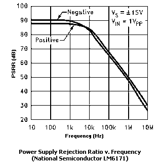
Figure 1c
Power-supply errors occur when noise from the power supply mixes with the input signal. The PSR (power supply rejection) specification is a measure of how well an opamp is able to block power supply noise and values of 100dB or more are common. PSR will vary with frequency, but the spec usually refers only to DC behavior. Instead, search for a graph in the datasheets of the PSR over the audio frequency range. In addition to choosing opamps with high PSR over a wide audio range, power-supply errors can be reduced by using power supplies that are highly regulated and bypassed.
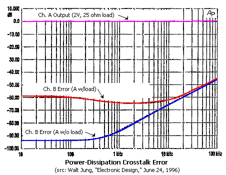
Figure 1d
Opamp-based headphone amplifiers can be prone to thermal errors due to output loading of the opamps. The power dissipation in an opamp when driving low impedance loads can raise the temperature of the device and cause changes in the input offset voltage, thus compromising the linearity. In dual and quad IC devices, the thermal conditions of one opamp can affect all others in the package because the opamp circuits share a common substrate ("power-dissipation-related crosstalk").
Thermal errors can be measured by comparing the output distortion of an opamp under load and no-load conditions. Figure 1d shows the thermal loading effect of one buffer on the other in a dual buffer IC (the system circuit is similar to figure 5d). Channel A is being fed a frequency sweep signal; channel B is idle. When buffer A is driving a 25 ohm load (as opposed to driving no load), it induces a stronger thermal-related error signal at the input of buffer B.
When the dual (or quad) IC buffers are used in circuits with voltage gain front-end as seen in figure 5d, these thermal errors can be corrected via global feedback. Conversely, buffering an input-stage opamp can reduce thermal errors in the input stage by isolating the power dissipation to the output stages. (For more information about buffering, see the section on output stages below.) In general, using single opamps instead of duals or quads will prevent power-dissipation crosstalk distortion. Precision low-noise opamps appear to have the lowest thermal errors.
TUBE-BASED OPAMPS
Unlike transistor amplifier design, tube amplifier design is more dependent on the electrical characteristics of the tubes themselves. Tube opamps attempt to bring the simplicity and higher preformance of amp-block design to tube audio. In audio applications, they can aspire to the same high performance as their solid state cousins and have the additional benefit of even-order distortion harmonics. There has been a revival of interest in these devices with the publication in recent years of several amp-block circuits, ranging from basic AC feedback amplifiers to tube-MOSFET hybrids - all configurable with the familiar opamp feedback scheme.
Not widely available back in the heyday of glass audio, tube opamps are very hard to find today. The following circuits develop the tube amp-block concept with increasing complexity. They all have limited current output and may need an output buffer stage to comfortably drive headphones (see the section on output stages below). To adjust the closed-loop gain of any of these amp-blocks, simply add a feeback resistor from the output to the inverting input and an input resistor - just as with solid state opamps. Some of these amp-blocks may prefer higher magnitudes of resistance than are typical of solid state opamps, so sample gain resistances are included. It's a good idea to construct several of these at a time to have a handy supply for experimentation.
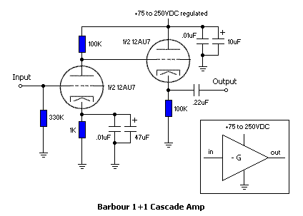
Figure 2
Eric Barbour's "1+1 Cascade" amp-block is an AC feedback amplifier (figure 2), consisting of a common cathode gain stage and a cathode follower output stage. This amp-block has a single inverting input and limited open loop gain, but is entirely suitable as a front-end of a headphone amplifier. The open loop figures are less than spectacular: G ~ -50, Fh ~ 30 kHz, THD > 2%, Rout ~ 2K ohms. When configured for a closed loop gain of -10 (Rf = 100K ohms, Rin = 10K ohms), the situation changes dramatically: Fh > 100 kHz, Rout ~ 500 ohms and THD drops below 0.4%. Since the 12AX7 is a dual triode, this design uses only 1 tube per channel. 12AU7s can also be subsituted, but the open loop gain will be lower. Purists may want to add an inverting output stage for correct output phase.
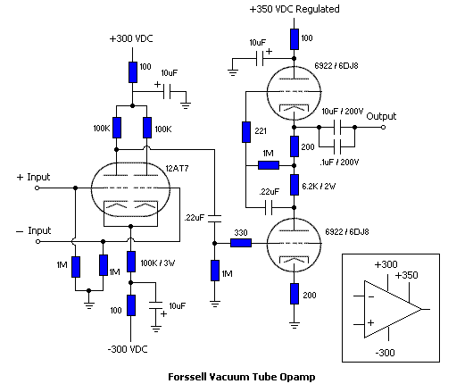
Figure 3
Fred Forssell's circuit (figure 3) has the differential input stage of a true opamp with a high common-mode rejection ratio (CMRR) and a mu follower output stage (biased at 12mA). The open loop gain is about 510 (30 from the first stage, 17 from the second). When configured for a closed loop gain of 18, the performance approaches that of solid state opamps: THD < 0.1%, Rout = 8 ohms, Fh > 400 kHz and s/n ratio = -86dB. Despite the low output impedance, the load impedance should be 3K ohms or greater to avoid increased distortion. When configuring this opamp for gains of less than 18, Forssell recommends using a lower mu input tube such as the 12AU7A for a lower open loop gain, so that less feedback is required.
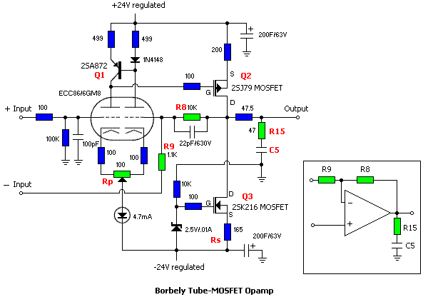
Figure 4
Both of the Barbour and Forssell amp-blocks use high voltage supplies, and neither is DC-coupled. Erno Borbely's hybrid design (figure 4) is both low voltage and DC-coupled. The differential input stage uses a single ECC86/6GM8 dual triode, which has a maximum anode voltage of 25V (a good substitute is the 6DJ8/ECC88). The current mirror Q1 and the constant current diodes (D1A and D1B) increase the CMRR and improve linearity. The output stage is a P-channel MOSFET configured as a common source amplifier with Q3 as its current source (the bias current is 10mA and can be adjusted by varying Rs). Rp is adjusted for 0 output voltage.
C2 provides phase compensation and if the opamp is configured for less than 6dB of gain, the R15-C5 low pass network must be added for stability (for G = 6dB, C5 = 100pF; for G = unity, C5 = 330pF). The open loop characteristics of the Borbely hybrid are excellent, especially for a tube opamp: G ~ 53dB, Fh ~ 90kHz and THD < 1%. When set to a gain of 10 (Rf = 10K ohms, Rin = 1.1K ohms), the specs once again are excellent: Fh > 700 kHz, THD < 0.1% and the output impedance is 50 ohms. A high load impedance (10K ohms) is recommended for maximum voltage output (15V).
CONFIGURING OPAMPS FOR VOLTAGE GAIN
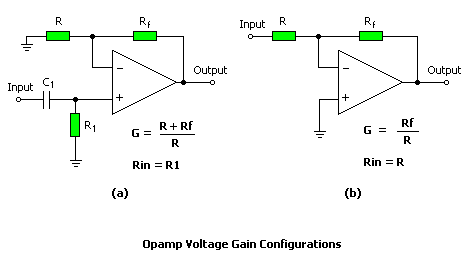
Figure 5
Opamps are most commonly used as voltage gain stages. The basic voltage-gain configurations are shown in figures 5a, 5b. The input impedance is the value of the input resistor. The output impedance Zo depends on the particular opamp, but generally decreases with decreasing gain (see the opamp datasheet for output impedance specs). If the opamp will be driving headphones directly, the output impedance should be less than 1/10th the headphone impedance across the audio spectrum. When choosing between inverting or non-inverting stage, the goal to keep in mind is that the opamp's contribution should result in correct phase at the amplifier output. As a rule of thumb, non-inverting configurations tend to have lower noise, higher input impedance and wider bandwidth, but may be subject to certain design constraints (see manufacturer specifications).
Headphone amplifiers are usually fed from the outputs of a preamp or portable stereos which have plenty of voltage gain (instead, they lack the current capability to drive headphones cleanly). If a headphone amplifier has a voltage gain stage, the gain is typically set between 2 and 10. Some opamps sound cleaner at lower gains. The feedback resistor Rf probably should be less than 1M for optimal stability (check manufacturer specs for other feedback network design issues), and lower feedback network impedances (Rf||Rin) result in lower noise.
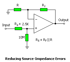
Figure 5c
Modern opamps do just fine with the basic configurations, but there are many design tweaks that can improve performance. One such optimization reduces source-impedance input errors in JFET-input opamps, which were discussed in the section on selecting opamps above. Recall that source-impedance input errors affect non-inverting gain configurations only and are caused by unequal source impedances at the + and - opamps inputs. The non-inverting amplifier in figure 5c balances the source impedances by choosing Rs = Rf||R. In a headphone amplifier, Rs is likely to be variable, in the form of a volume control, and so the 2K to 3K value is an approximation.
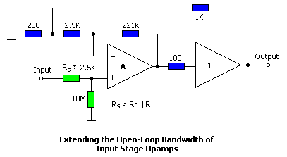
Figure 5d
In a multi-stage opamp system (such as a voltage gain stage followed by a current buffer - see the section on output stages for more information), if the input stage opamp has a bipolar input stage and narrow open-loop bandwidth, it may exhibit nonlinearities when fed high level, high frequency signals. The system in figure 5d has an input stage opamp, which has had its open-loop bandwidth effectively extended under local feedback. The overall gain of the system is 5, but the local gain of the input stage is about 100 for an effective open-loop bandwidth of 100kHz. The bandwidth extension should go well beyond the audio range.
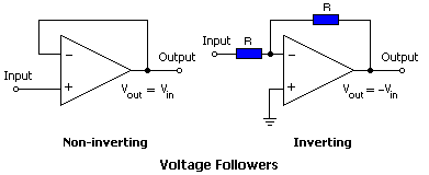
Figure 6
If the opamp is configured for a gain of 1 (R = Rf), it becomes a voltage follower. Most solid state opamps will also function as non-inverting followers with a straight wire in place of the feedback resistor (figure 6). Non-inverting voltage followers have the input impedance and a low output impedance. The input impedance of an inverting follower is the resistance of the input resistor. Voltage followers are often used as buffers which could drive headphones, but voltage gain opamps have modest current capability. A high current buffer opamp is specially designed to provide large amounts of current - perfect for driving headphones. For more information, see the section on output stages below.
Handling Balanced Inputs
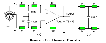
Figure 7
Pro audio equipment may have balanced inputs and outputs - where the ground is separate from the signal ground for more effective noise shielding. Thus, each channel has a total of 3 connections: signal, signal ground and ground. A headphone amplifier is only concerned with handling balanced inputs. The circuit in figure 7 converts a balanced input into a single-ended signal with unity gain (the input resistors are split to implement a RF filter - see below). The resistors must be matched to within 0.1% or the CMRR will degrade (e.g., an 80dB CMRR can drop to 60dB due to input resistor mismatch). The converter can also be configured with gain determined by the ratio of Rf / R, but keeping all Rs that same value makes matching the resistor array easier.
AC Coupling and RF Input Filters
Bandwidth-limiting the signal input can block DC voltages or filter out RF noise. DC protection is not necessary if the audio source already has 0 DC output, but some designers prefer extra insurance. With values of 1uF and 100K, the high-pass input filter in figure 5a has a corner frequency of about 1.6Hz and will minimally affect bass response or overall sound quality - if a high quality parts are used (e.g., film capacitors and metal film resistors). Instead of the resistor, an audio taper potentiometer could be substituted to serve as a volume control.
If the signal has RF noise, it can be cleaned up with a low-pass filter at the inputs. The low-pass network in figure 7a has a corner frequency of about 200kHz. An alternative RF network is shown in figure 7b. Frequencies above the corner frequency are mixed together, so that they are canceled out by the opamp's CMRR. As with the resistor array, the RF capacitors should also be matched as closely as possible. Also use shielded cable when wiring the inputs to further reduce noise pickup.
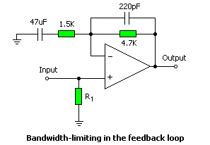
Figure 8
Low and high pass filters can be cascaded at the input, so long as the resistor values of each filter are different by at least a factor of 10. Also, the impedance of input network will affect the overall impedance of the input stage, so must be accounted for in selecting filter resistance values. These bandpass filters can alternatively be incorporated into the feedback loop. The circuit in figure 8 has an approximate bandpass from 2Hz to 150kHz. Some audiophiles may be able to hear distortion from capacitors in the signal path. As with opamp distortion, capacitor distortion is not audible to everyone. Before discarding the benefits, audition the amp on a protoboard with and without the capacitors.
THE OUTPUT STAGE
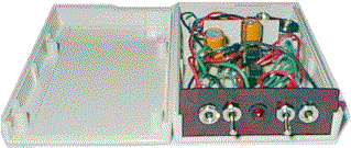
Voltage-gain opamps may output enough current to drive some headphones directly (check the manufacturer specs). For example, the author built a pocket headphone amp (shown above) with Burr-Brown OPA132 opamps in a non-inverting configuration as shown in figure 5. The amp has no trouble reaching ear-splitting volumes with most headphones. For more information about this project, see A Pocket Headphone Amplifier. Modern dynamic headphones will play loudly with just a few milliwatts (see Understanding Headphone Power Requirements).
However, when an opamp does not have enough current capability or if it is susceptible to output loading errors (for information on output loading errors, see the section on selecting opamps above), it must then be augmented by an output stage. This section reviews solid state and tube class A followers, class AB symmetric emitter followers and buffer opamps (which are nothing more than elaborate emitter followers) as output stages. For tube amp-block front-ends, there is a discussion on interfacing tubes to solid state output stages. Note: the class A followers and high current buffers described below also make excellent standalone headphone amplifiers, where voltage gain is not necessary.
Class A MOSFET Follower
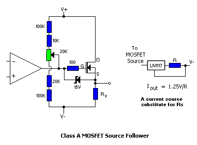
Figure 9
Purists prize class A amplifiers as capable of reproducing audio signals with the ultimate fidelity, because the output voltage swing is under the control of a single transistor or tube. Class A amplifiers are inefficient, consuming up to 400% more power than they output, but are enjoying revived popularity for their simple topologies (especially single-ended class A amps). Whereas class A loudspeaker amps run hot enough to heat a room, headphone fans can indulge without guilt, since headphones require very little power.
The MOSFET source follower in figure 9 is a single-ended class A output stage. MOSFET followers (and their bipolar cousins, emitter followers) are current amplifiers, which have non-inverting unity (or slightly less than unity) gain. A voltage divider biases the MOSFET. The bias pot Rp adjusts the output voltage to 0V for DC coupling (see Greg Szekeres' Class A Headphone Driver for an AC coupled design). An input coupling capacitor is necessary only if the previous stage has a DC offset.
The transistor can be any power MOSFET, so long as the voltage and current ratings are adequate. MOSFETs have the "soft" overload characteristics of vacuum tubes and are preferred in this type of application over bipolars. The gate resistor helps to stabilize the MOSFET, and the zener protects the gate from voltage transients. The VDS spec must be higher (at least twice) the idle voltage, which is usually about 1/2 the total supply voltage. Rs is a power resistor and determines the idle current. Starting with an idle current of about 100mA and -V = -15V, then Rs = 15/.1 = 150 ohms. The resistor's power rating should be much greater than 15 * 0.1 = 1.5W (at least 3W to be safe). Also make sure that the MOSFET is heatsinked to dissipate a similar amount of power.
Instead of a resistor for Rs, a precision current source would improve linearity. Current sources are usually made with a transistor, but the version in figure 9 employs a LM117/317 floating regulator, which needs only one resistor to adjust current output from 10mA to 1.5A. The voltage differential between Vin and Vout (which is the 1.25V internal reference voltage) should be between 7 and 15V. At higher differentials, the current output starts dropping due to internal safe-area protection, in which case more than one current source can be paralleled for higher output. While not required, the output capacitor helps eliminate any instability. Again, heatsinking is recommended.
AC-Coupled Cathode Follower
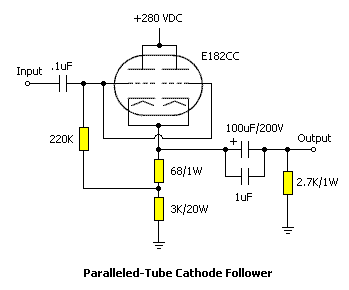
Figure 10
From a design point of view, tubes are less favored as output stages, because the output impedance is higher than can usually be achieved with transistors. Yet, there are many excellent headphone amps with tube outputs. The AC-coupled cathode follower in figure 10 (from Andrea Ciuffoli's headphone amp project) achieves a relatively low output resistance of about 33 ohms by paralleling two sections of a dual triode. The cathode resistor is tapped to provide self-bias. Each section is biased at 26mA or 52mA total.
The output impedance of a single-tube cathode follower is calculated as: Zout = Rk / (1 + GmRk), where Gm is the tube's transconductance and Rk is the total resistance of the cathode resistors. Therefore, when building a cathode follower, select tubes with a high transconductance to get the lowest output impedance.
Class B and AB Symmetric Emitter Followers
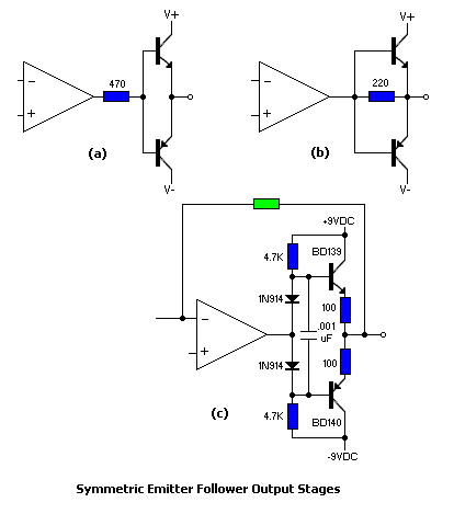
Figure 11
The high power consumption of class A amplifiers makes them impractical in battery-powered headphone amplifiers. The current booster circuits in figure 11 have complementary output devices that each reproduce one half of the audio signal. These schemes are more efficient because the idle current can be very low or even 0mA. The circuit in figure 11a is a class B amplifier with Q1 and Q2 off at turned off at idle. When the audio signal is positive, Q1 conducts; when it is negative, Q2 conducts. However, both transistors conduct only when the signal exceeds the forward bias voltages which is around 0.7V. Therefore, both transistors remain off when the audio signal is between ±0.7V, resulting in crossover distortion at the output. Since headphones are driven at low output voltages, this type of distortion is particularly noticeable in a headphone amplifier.
The circuit in figure 11b improves performance by allow the opamp stage to supply current until the voltage drop across R is large enough to forward bias both transistors. However, this design suffers from fluctuating output impedance. The output stage in figure 11c solves both problems by having both transistors conducting at very low idle currents. The voltage drop across the two diodes forward biases Q1 and Q2; the emitter resistors determine the idle current - about 0.6mA with these values. The output stage operates in class A at low levels - until the load draws more current or voltage swing than one of the transistors can provide. For battery operation, the output stage is often biased from 1-10mA, trading off between sound quality and battery life. The minimum idle current is best determined by monitoring a sine wave output on an oscilloscpe while adjusting the bias until the crossover distortion just disappears. AC powered amplifiers can take advantage of extended class A operation by increasing the bias current. Earle Eaton's headphone amplifier uses a variation of this design. Sheldon Stokes' headphone amplifier has a class AB MOSFET output stage.
High Current Buffers
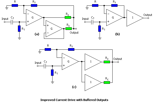
Figure 12
High current buffers are basically output stages on a chip. Because they are specialty products and are meant for use in specific applications, buffers are optimized to be particularly good at one job. In general, these chips have fantastic specs: slew rates in the hundreds, low distortion and of course, high current capability. For a headphone amplifier, a buffer that can output 100mA is probably more than sufficient, but additional current drive doesn't hurt, so long as the power supply requirements meet the builder's goals. Figure 12a shows a voltage gain opamp with its current capability doubled with the help of an identical opamp configured as a voltage follower. The load balancing resistors ( Rc ) are about 50 ohms. The output impedance of this circuit would be Rc || Rc || ( R + Rf ), but the impedance seen by the headphones is much less - reduced by the effect of the feedback taken at the outputs of the combined Rcs: Zout = Rout / amount of feedback.
Figures 12b and 12c show voltage gain opamps augmented with current buffers - 12b has a buffer outside the feedback loop and 12c has buffers inside. The overall gain for both versions is the same, but the version with global feedback might function with greater linearity. However, some designers argue that these buffers are already very linear, and global feedback can introduce instability into a system. Both configurations work. If the circuit of figure 12c is wired for local feedback only, such as in figure 12b, then the load balancing resistors can be as little as 1 ohm for a lower output impedance. When using dual or quad buffer ICs, global feedback can help correct for output loading errors (see the sections on selecting opamps and configuring opamp voltage gain stages for more information about output loading errors).
Note: Class A output stages can similarly be excluded from the feedback loop, but class AB stages should be included, since they are more prone to nonlinear operation.
In the case where a single buffer does not supply enough current or has an output impedance that is too high, it is possible to parallel output buffers. Figure 12c doubles output current capability and cuts output impedance in half by paralleling 2 output buffers. The current-summing output resistors Rc (typically 50 ohms) ensure that all of the buffers contribute equally to the output. Again, because the feedback is taken after the Rcs, the output impedance seen by the headphones is less than 1 ohm. Ben Duncan's PHONES-01 headphone amplifier substitutes ferrite beads and incandescent lamps (see below) for the output resistors, reasoning that any unequal sharing is likely to be in the RF range. The beads also help block RF. Again, the feedback loop can be placed either before or after the parallel buffers.
Interfacing Tubes To Solid State Output Stages
When interfacing tubes with solid state output stages, the higher operating voltages of tubes pose two potential problems. First, the power supply may have to be "stepped down" and second, tube circuits can send out high voltage transients that could damage solid state components. The solutions: use high voltage opamps and buffers and/or limit the voltage going into solid state inputs. With a high-voltage MOSFET, the class A source follower described above would interface well with tube gain stages, as tubes and MOSFETs have similar sonic characteristics. The MOSFET amp has zener protection against overvoltage damage. There are also high-voltage bipolar devices, but they are less common. Apex Microtechnologies and Burr Brown are two manufacturers of high voltage opamps and buffers. Many of these are well-suited for audio applications, and a few chips are able thrive on power supplies of up to ±600V.
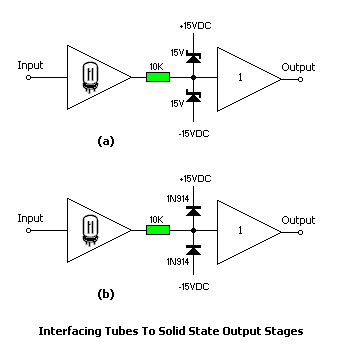
Figure 13
High voltage output stages may also have input voltage limitations that tubes could breach. The following are two overvoltage protection schemes that can be used with any solid state output stage. Figure 13a is a suggestion by Eric Barbour. When fed high voltage transients, the zeners clamp the input to a maximum of ±15V. Figure 13b is the protection scheme that Greg Szekeres uses in his MOSFET headphone driver. Here, transients in excess of the power supply voltages will forward bias the silicon diodes and be conducted out of the system. The input resistor sets the minimum load impedance seen by the tube output.
Output Current Limiting
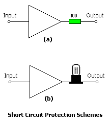
Figure 14
When a headphone plug is inserted or removed from the jack, the possibility arises that the amplifier outputs will be shorted, if only briefly. Without current limiting, such a short could burn out opamps and/or output stage transistors. Rather than resort to complex current sensing schemes, figure 14 shows two common limiting mechanisms that protect against short-circuit damage: current limiting resistors and incandescent bulbs. Current limiting resistors set the minimum load that the amplifier can see - typically 100 ohms, 1/2W. Output resistors will reduce the output power and increase the amplifier's output resistance, but most headphones will be unaffected. Another option is to locate the current limiting resistors inside the feedback loop (figure 12) so that the effective output impedance of the amplifier is minimized from the feedback. See Headphone FAQs for more information about the impact of amplifier output impedance on headphone sound.
In place of a current limiting resistor, an incandescent lamp has the advantage of very low resistance when the filament is cold. Lamp filaments have a positive temperature coefficient. As increasing current heats the filament, the resistance also goes up, thereby reducing the output current. Choose lamps with voltage and current characteristics similar to that of the output stage. Incandescent lamps were once popularly deployed to protect loudspeakers from overdrive. The idea resurfaced as output limiting for headphone amplifiers in Ben Duncan's PHONES-01 headphone amplifier project.
EQUALIZATION
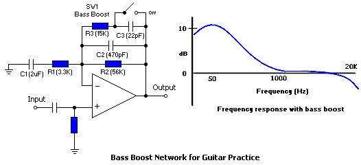
Figure 15
Designing an equalization stage is an entire subject by itself (see Designing a Pocket Equalizer for Headphones). Equalization can be implemented in separate circuit blocks - either as active stages or passive networks - to ensure that they can be switched out completely without compromising the quality of the main gain stage. But there are instances where equalization is so important and basic to the use of the amplifier that the EQ filter network is incorporated in the feedback loop of the main gain stage for convenience and economy. For example, headphone amplifiers for guitar practice almost always require a bass boost.
Figure 15 shows a bass boost feedback network by T. Giesberts that gives a 10dB boost at 50 Hz when turned on. The network is a shelving EQ. With the boost deactivated, R1-C1 and R2-R3-C2 form a bandpass with threshold frequencies of about 20Hz and 30kHz. The gain of the amplifier is determined by (R2 || R3)/R1 and is approximately 4 with the values shown. With the boost switched in, R3-C3 create a bass shelf, with a threshold frequency of about 500Hz. The downturn in the low frequency response below 50Hz is caused by the attenuation from the input high pass filter.
ACOUSTIC SIMULATION
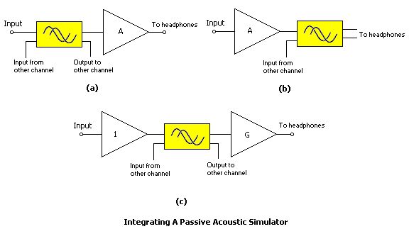
Figure 16
Headphone sound suffers from a "super-stereo" effect caused by the isolation of each audio channel to one ear. Acoustic simulators electronically alter the stereo signal to create a more natural soundfield in headphones. They may be implemented with digital or analog filters (also called crossfeed filters). While digital and active analog simulators have amplification for headphones built into the design, passive simulators are RC networks that shape and time delay the crossfeed. Passive networks are sensitive to the source and load impedances that can affect the frequency response of the networks. (For examples of passive acoustic simulators, see the HeadWize Projects Library. For more information about digital and active network simulators, see Technologies for Surround Sound Presentation in Headphones.)
Depending on the input and output impedances of a passive simulator, it can appear at the input or output of a headphone amplifier (figures 16a, 16b), but isolating the network between two amplifier stages will often result in the best performance (figure 16c). With two isolating stages, the network can be assured of seeing a low input source impedance and a high output load impedance, such that the frequency response of the network remains constant. Both stages can be voltage gain blocks and/or unity-gain buffers, as the application may require.
However, with battery-powered amplifiers, which may operate the opamps at lower voltages, the preferred way to construct a headphone amplifier with an acoustic simulation is to make the second stage a voltage gain block to compensate for any insertion loss through the network as well as provide for overall voltage gain. If the voltage-gain block does not output sufficient current to drive headphones, add a high current, unity-gain buffer after the voltage-gain block.
When using multiple opamp gain stages, be sure to check the idle voltage at the output of the last stage. If it is more than a few millivolts, the DC-offset voltages of the opamps must be adjusted - either by trimming the DC offsets, by adding capacitors between stages and at the output to block offsets or by selecting feedback resistors to minimize offsets (see next section).
ADJUSTING DC-OFFSET VOLTAGES IN MULTI-STAGE AMPLIFIERS
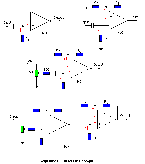
Figure 17
In single stage amplifiers, the opamp's DC offset voltage is only a few milliamps and is rarely a problem. In multistage amplifiers, DC offsets may be amplified by successive stages until the idle voltage at the output of the final stage reaches several volts, although the overall gain the system may not be very high. Jan Meier experienced this situation while building and testing a headphone amplifier:
Referring to figure 17a, the non-inverted input of an opamp wired as a voltage follower requires a small input bias current (i+) that, since it flows through the resistor R1, generates a non-zero voltage V+ = (i+)*R1 at the input. Typical values for i+ are 1uA to 2uA (LM6171/LM6181/LTC1206) for bipolar-input, or 1 to 50 pA (OPA627/OPA604) for FET-input amplifiers. With a R1 of 100K, V+ (and thus Vout) can have values up to 200 millivolts!
In figure 17b, a feedback loop is added that amplifies V+ by a factor (R3+R2)/R2. It is not unusual for a headphone amplifier to have a gain factor of around 5. This will, however, also amplify V+ for a Vout of up to 1000mV, which can damage headphones - especially low impedance headphones. Fortunately the inverted input also generates a bias current (i-) that generates a DC-voltage (V-) at the inverted terminal and thus counteracts the effects of V+. The effective resistance to ground seen by the inverted input is the value of R2 and R3 in parallel which equals (R2R3)/(R2+R3). To eliminate the output voltage offset generated by i+, the input voltage V- should be equal to V+:
(i+)R1 = (i-)*(R2R3)/(R2+R3)
To select values for R2 and R3, first take a look at the specifications of the opamp for i+ and i-. Note that they do not have to have the same value. For instance, the LTC1206 has an i+ value of 2uA whereas i- goes up to 10uA! By a proper selection of the resistor values, the offset can be strongly reduced. With a headphone amplifier made from a LM6171 opamp and having R1 = 47 kOhm, R2 = 56 kOhm, R3 = 300 kOhm, one channel shows a very good offset of only 20 mV. The other channel came down to a hardly measurable 0.2 mV! The fact that the channels were not equal simply has to do with manufacturing variations in opamps of the same type.
A problem remains with the input stage. If the input potentiometer is directly coupled to the opamp, the value of R1 now changes with the volume control, and a perfect fit of the resistances can not be made. A possible solution is shown in figure 17c. The resistance of the potentiometer no longer has an influence on the DC-resistance of the opamp. Alternatively, if the headphone amplifier has a second stage, the input stage can be decoupled from the second stage as shown in figure 17d. If the output of a first stage is directly coupled to the input of a second stage, the effective value of R1 is zero and a match can not be made. However, you simply can put a resistor between output and input.
Last warning: If the headphone amplifier will also be a preamplifier, any DC-offset at the output will be amplified by the power amp and will be fed into a low resistance loudspeaker. In this situation a few millivolts offset can damage the loudspeaker. To prevent any damage to loudspeakers or to the power amp, always use (decent quality) capacitors at the output of the preamp.
HEADPHONE DISTRIBUTION AMPLIFIERS
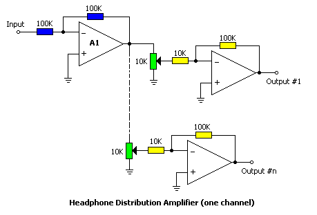
Figure 18a
Multitrack recording allows musicians to record songs in layers. Tracks can be added or overdubbed. Musicians may be positioned far apart from each other or play at different times to isolate their performances for the greatest flexibility in editing. Headphone monitoring is the most common way for musicians to hear each other under these circumstances, and a headphone distribution amplifier is central to this function.
Headphone distribution amplifiers can drive several pairs of headphones from a single set of inputs. While it is fairly easy to build one from a power amplifier with a ladder of output resistors (see the headphone FAQs for instructions), there are advantages to driving each headphone from its own amplifier, such as greater control over gain. The first stage of the basic distribution amplifier shown in figure 18a is a voltage follower that provides impedance buffering and signal inversion for correct phase at the headphone output. The buffer feeds any number of headphone amplifier blocks with their own volume controls.
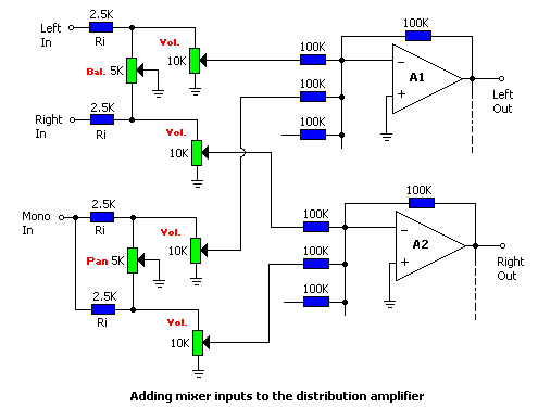
Figure 18b
As more musicians demand custom mixes, so commercial distribution amplifiers have begun adding mixer features. Figure 18b shows how to convert the input buffer stage of the basic distribution amplifier into a mixer stage. The input buffers (A1 and A2 for the left and right channels) now have a series of 100K summing resistors, one resistor for each stereo or mono input. The level controls for the stereo and mono inputs are balance-volume and pan-volume sets of pots. To move the balance or panning characteristic closer to the ends of the pot rotation, decrease the value of Ri.
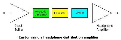
Figure 18c
A full-featured headphone distribution amplifier will have limiters and possibly equalization stages for each headphone output. An acoustic simulation network, equalizer and/or limiter can be placed between the buffer and headphone amplifier blocks (see Designing a Limiter for Headphone Amplifiers for information about limiters and Designing a Pocket Equalizer for Headphones for equalization schematics). To increase the drive capability of an amp block, add a current buffer output stage (after any active EQ stages).
POWER SUPPLIES
AC Power Supplies
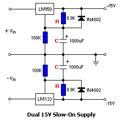
Figure 19
To regulate or not to regulate, the answer depends on the circuit. Modern opamps have excellent power supply rejection ratios (PSRR) and are less affected by voltage fluctuations than older products, but discrete output stages may be more vulnerable. Since headphone amplifiers draw so little power and 3-pin regulators are cheap, it cannot hurt to have a regulated supply. Figure 19 shows a dual supply with the LM150/LM133 floating regulators configured for slow-start to minimize turn-on thumps. The delay is R*C = 8900 * 1000 E-6 = 9 seconds. Also check for power supply schematics in HeadWize Projects articles or in the datasheets for regulators. In any case, each opamp should be decoupled from the power supply with a 0.1uF ceramic capacitor and possibly a 10uF electrolytic, connected from the power supply pins to ground (see figure 14e below).
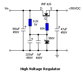
Figure 20
Tube circuits often do not use regulated supplies, but where recommended, it is usually a single high voltage regulated supply for a gain stage and/or a low voltage regulated supply for tube heaters. For example, the Forssell tube opamp requires a regulated +350V supply for the output stage (at least 30mA for two opamps) and a 6V regulated supply for the heaters to minimize hum. Floating regulators, such as the LM150, can output hundreds of volts, so long as the input/output differential voltage remains within spec (and don't forget to diode protect the regulator). Figure 20 shows a simple zener-based high voltage regulator. If the output voltage goes up, the potential across VGS decreases and the MOSFET reduces output current. If the output voltage goes down, then VGS increases, and output current increases. The IRF420 specified has a VDS of 450V and an ID of 2A continuous and must be mounted on a heatsink. The zener can be any series of 5W zeners (for the Forssell circuit) that total about 350V.
Battery Supplies
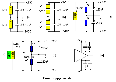
Figure 21
There are opamps that will operate on a single 1.5V cell. Such micro-power opamps can drive very efficient, low-impedance headphones. With other headphones, the inability of micro-power opamps to develop higher voltages across the load will limit the volume. One method of getting higher voltages from batteries is to stack the batteries in series. Another is to raise the battery voltage with a DC-to-DC converter (to several volts or even several hundred volts in the case of portable electrostatic headphones). DC-to-DC converters, also called switching regulators, do their magic by changing the DC voltage to an AC voltage via an oscillator, which feeds a step-up transformer or capacitive/inductive reservoir to build the voltage, and then is converted back to DC at the higher voltage. As with any AC-based supply, a DC-to-DC supply must have a good filter network at the output to minimize power supply noise.
Opamps can run off single supplies, but are designed for dual supplies. Headphone amps with direct-coupled outputs must be powered from dual supplies. If there is room in the amplifier enclosure, separate batteries for the positive and negative supplies is the suggested implementation (figures 21a, 21b). If the opamp can run on a supply of ±3V or less, a single 9V battery can be converted into a dual supply as shown in figure 21c. A voltage divider creates a virtual ground at the center junction and draws less than 1 ma. at idle. The electrolytic ouput capacitors both reduce the supply impedance at high frequencies and function as a power reservoir to simulate two separate battery sources.
This version of a virtually grounded supply works best with amplifiers that draw lower idling current, as the capacitors must be able to "recharge" quickly. Start with 100uF capacitors. With an oscilloscope or a multimeter, monitor the supply for any ringing or fluctuation with the amplifier driving headphones loudly. Increase the capacitance or decrease the resistor values of the voltage divider to compensate (decreasing the voltage divider resistance values will increase idle current). The most important test of all is the listening test. Despite supply fluctations, the amplifier may function without audible detriment. For a simple AC power supply, apply this circuit to an adapter with 6V regulated output (Radio Shack sells one) to get regulated ±3V (figure 21d). Regardless of the supply option used, decoupling the opamps from the supply (figure 21e) will improve stability.
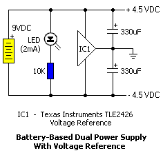
Figure 22
There may be times, though, when a virtually-grounded dual supply has a tendency to "rail" when the resistor-type voltage divider cannot maintain the virtual ground at 1/2 Vcc. Such cases may occur when the opamp draws too much current or input signal (for example, a high boost equalizer) pushes the opamp into heavy clipping and power supply is unable to recover. There are several inexpensive commercial voltage references that can output a stable 1/2 Vcc regardless of the load. Figure 22 shows a virtually-grounded dual supply implemented with the Texas Instruments TLE2426 voltage reference and one 9V battery (the TLE2426 is excellent also with two 9V batteries for a stable, dual 9V supply). Before selecting a voltage reference, check the specifications to see if it has adequate current capability for the load.
Addendum
11/11/98: Expanded discussion of using opamps to drive headphones directly without an output stage. Also updated figures 21c, 21d - lowered voltage divider resistor values to 5K, based on experimentation.
11/13/98: Added image and description of pocket headphone amp.
5/10/99: Added the following new sections: Equalization, Acoustic Simulation, Adjusting Opamp DC-Offsets. Also, minor revisions in other sections.
7/19/99: Added section on headphone distribution amplifiers.
7/20/99: Updated section on headphone distribution amplifiers.
7/24/99: Updated section on headphone distribution amplifiers.
1/3/00: Updated the following sections: Selecting Solid State Opamps, Configuring Opamps for Voltage Gain, The Output Stage.
1/24/00: Corrected reversed opamp input connections in figure 18a and 18b. Also corrected calculation of Rs for MOSFET driver in figure 9.
4/10/00: Revised figure 16c and corresponding description.
References:
___, Electronic
Circuit Design Handbook, 1971.
___, National Semiconductor Audio/Radio Handbook (1986).
___, "Applications For An Adjustable IC Power Regulator," National
Semiconductor, January 1997.
___, "BUF634 Application Notes," Burr-Brown, 1993.
___, "LF353 Application Notes," Texas Instruments, 1993.
___, "NE5532 Application Notes," Philips Semiconductor, April 1996.
___, "MLM82 Mixer Schematic," Rane Corporation, May 1998.
___, "LM150 Application Notes," National Semiconductor, May 1998.
___, "LM358 Datasheet," National Semiconductor, Sept. 1999.
___, "LM6171 Datasheet," National Semiconductor, May 1998.
Banks, Morgan, "AB-051 Double The Output Current To A Load With The OPA2604 Audio
Opamp", Burr-Brown, 1993.
Barbour, Eric, "Vacuum Tube AC Feedback Amplifiers," Glass Audio, 2/92.
Barbour, Eric, "1 + 1 Cascade Amplifier," Glass Audio, 6/92.
Borbely, Erno, "Low-Voltage Tube-MOSFET Line Amp," 1/98, p. 1.
Danner, Denzil G., "Tube Circuit Primer: A Reference," Glass Audio, 3/92, p. 20.
Duncan, Ben, "How Clean Is Your Opamp," Electronics World + Wireless World,
January 1993, p. 42.
Duncan, Ben, "Phone Home," Hi-Fi News and Record Review, May 1997, p. 68.
Duval, Bernard, "IRF150 Hybrid Amp," LED, Winter 1996.
Fox, Harry, Master OpAmp Application Handbook, 1978.
Forssell, Fred, "A Vacuum Tube Op Amp," Glass Audio, 1/95, p. 1.
Giesberts, T., "Headphones Amplifier for Guitarists," Elektor Electronics,
11/96, p. 32.
Horowitz, P. and Hill, W. The Art of Electronics (1989).
Jung, W., Audio IC OpAmp Applications (1988).
Jung, W., "Composite Line Driver With Low Distortion," Electronic Design,
6/24/96, p. 78.
Jung, W., Minimizing Input
Errors, Electronic Design, 12/14/98.
Jung, W., Realising High
Performance: Bandwidth Limitations, Electronic Design, 12/1/98.
Jung, W., Realising High
Performance: Buffers (Part 1), Electronic Design, 9/1/98.
Jung, W., Realising High
Performance: Buffers (Part 2), Electronic Design, 10/1/98.
Pass, Nelson, "DIY Opamps," Audio Electronics, 6/98.
Pass, Nelson, "The Bride of Zen," Audio Amateur, 4/94.
Pass, Nelson, "The Pass Zen Amplifier," Audio Amateur, 2/94.
Pass, Nelson, "Zen Revisited," Audio Amateur, 3/94.
Van Alstine, Frank, "The AVA Versa-Kit Headphone Amplifier Do-it yourself
Project," Audio By Van Alstine Website, 9/97.
Also thanks to Richard
Steven Walz for his insight on virtually-grounded dual power supplies.
c. 1998, 1999, 2000 Chu Moy.